Top Qs
Timeline
Chat
Perspective
Zen 2
2019 AMD 7-nanometer processor microarchitecture From Wikipedia, the free encyclopedia
Remove ads
Zen 2 is a computer processor microarchitecture by AMD. It is the successor of AMD's Zen and Zen+ microarchitectures, and is fabricated on the 7 nm MOSFET node from TSMC. The microarchitecture powers the third generation of Ryzen processors, known as Ryzen 3000 for the mainstream desktop chips (codename "Matisse"), Ryzen 4000U/H (codename "Renoir") and Ryzen 5000U (codename "Lucienne") for mobile applications, as Threadripper 3000 for high-end desktop systems,[6][7] and as Ryzen 4000G for accelerated processing units (APUs). The Ryzen 3000 series CPUs were released on 7 July 2019,[8][9] while the Zen 2-based Epyc server CPUs (codename "Rome") were released on 7 August 2019.[10] An additional chip, the Ryzen 9 3950X, was released in November 2019.[8]
At CES 2019, AMD showed a Ryzen third-generation engineering sample that contained one chiplet with eight cores and 16 threads.[6] AMD CEO Lisa Su also said to expect more than eight cores in the final lineup.[11] At Computex 2019, AMD revealed that the Zen 2 "Matisse" processors would feature up to 12 cores, and a few weeks later a 16 core processor was also revealed at E3 2019, being the aforementioned Ryzen 9 3950X.[12][13]
Zen 2 includes hardware mitigations to the Spectre security vulnerability.[14] Zen 2-based EPYC server CPUs use a design in which multiple CPU dies (up to eight in total) manufactured on a 7 nm process ("chiplets") are combined with a 14nm I/O die (as opposed to the 12nm IOD on Matisse variants) on each multi-chip module (MCM) package. Using this, up to 64 physical cores and 128 total compute threads (with simultaneous multithreading) are supported per socket. This architecture is nearly identical to the layout of the "pro-consumer" flagship processor Threadripper 3990X.[15] Zen 2 delivers about 15% more instructions per clock than Zen and Zen+,[16][17] the 14- and 12-nm microarchitectures utilized on first and second generation Ryzen, respectively.
The Steam Deck,[18][19] PlayStation 5, Xbox Series X and Series S all use chips based on the Zen 2 microarchitecture, with proprietary tweaks and different configurations in each system's implementation than AMD sells in its own commercially available APUs.[20][21]
Remove ads
Design
Summarize
Perspective


Two delidded Zen 2 processors designed with the multi-chip module approach. The Ryzen 5 3600 CPU on the left/top (used for mainstream Ryzen CPUs) uses a smaller, less capable I/O die and one CCD (the space for an additional CCD is used on the Ryzen 9), while the Epyc 7702 on the right/bottom (used for high-end desktop, HEDT, Ryzen Threadripper and server Epyc CPUs) uses a larger, more capable I/O die and up to eight CCDs.
Zen 2 is a significant departure from the physical design paradigm of AMD's previous Zen architectures, Zen and Zen+. Zen 2 moves to a multi-chip module design where the I/O components of the CPU are laid out on its own die which is separate from the dies containing processor cores, which are also called chiplets in this context. This separation has benefits in scalability and manufacturability. As physical interfaces don't scale very well with shrinks in process technology, their separation into a different die allows these components to be manufactured using a larger, more mature process node than the CPU dies. The CPU dies (referred to by AMD as core complex dies or CCDs), now more compact due to the move of I/O components onto another die, can be manufactured using a smaller process with fewer manufacturing defects than a larger die would exhibit (since the chances of a die having a defect increases with device (die) size) while also allowing for more dies per wafer. In addition, the central I/O die can service multiple chiplets, making it easier to construct processors with a large number of cores.[15][22][23]

@Zen2@Rome@EPYC_7702_ES@2S1404E2VJUG5_BB_ES_DSCx16_CCD_polysilicon@5xLED.jpg)
@Zen2@Rome@EPYC_7702_ES@2S1404E2VJUG5_BB_ES_DSCx13_IOD_polysilicon@5x.jpg)
@Zen2@Matisse@Ryzen_5_3600@100-000000031_BF_1923SUT_9HM6935R90062_DSCx8_IOD_polysilicon@5x.jpg)
On the left (top on mobile): Die shot of a Zen 2 Core Complex Die. On the middle: Die shot of a Zen 2 EPYC/Threadripper I/O die, On the right (bottom): I/O die of a Zen 2 mainstream Ryzen I/O die.
With Zen 2, each CPU chiplet houses 8 CPU cores, arranged in 2 core complexes (CCXs), each of 4 CPU cores. These chiplets are manufactured using TSMC's 7 nanometer MOSFET node and are about 74 to 80 mm2 in size.[22] The chiplet has about 3.8 billion transistors, while the 12 nm I/O die (IOD) is ~125 mm2 and has 2.09 billion transistors.[24] The amount of L3 cache has been doubled to 32 MB, with each CCX in the chiplet now having access to 16 MB of L3 compared to the 8 MB of Zen and Zen+.[25] AVX2 performance is greatly improved by an increase in execution unit width from 128-bit to 256-bit.[26] There are multiple variants of the I/O die: one manufactured on GlobalFoundries 14 nanometer process, and another manufactured using the same company's 12 nanometer process. The 14 nanometer dies have more features and are used for the EPYC Rome processors, whereas the 12 nm versions are used for consumer processors.[22] Both processes have similar feature sizes, so their transistor density is also similar.[27]
AMD's Zen 2 architecture can deliver higher performance at a lower power consumption than Intel's Cascade Lake architecture, with an example being the AMD Ryzen Threadripper 3970X running with a TDP of 140 W in ECO mode delivering higher performance than the Intel Core i9-10980XE running with a TDP of 165 W.[28]
New features
- Some new instruction set extensions: WBNOINVD, CLWB, RDPID, RDPRU, MCOMMIT. Each instruction uses its own CPUID bit.[29][30]
- Hardware mitigations against the Spectre V4 speculative store bypass vulnerability.[31]
- Zero-latency memory mirroring optimization (undocumented).[32]
- Doubled width of the execution units and load store units (from 128-bit to 256-bit) in the floating point coprocessor and significant further throughput enhancements in the multiplication execution unit. This allows the FPU to perform single-cycle AVX2 calculations.[33]
- Introduced CPPC power management.[34]
Remove ads
Feature tables
CPUs
This section is empty. You can help by adding to it. (March 2023) |
APUs
Products
Summarize
Perspective
On 26 May 2019, AMD announced six Zen 2-based desktop Ryzen processors (codenamed "Matisse"). These included 6-core and 8-core variants in the Ryzen 5 and Ryzen 7 product lines, as well as a new Ryzen 9 line that includes the company's first 12-core and 16-core mainstream desktop processors. [35]
The Matisse I/O die is also used as the X570 chipset.
AMD's second generation of Epyc processors, codenamed "Rome", feature up to 64 cores, and were launched on 7 August 2019.[10]
Desktop CPUs
3000 series (Matisse)
Common features of Ryzen 3000 desktop CPUs:
- Socket: AM4.
- All the CPUs support DDR4-3200 in dual-channel mode.
- L1 cache: 64 KB (32 KB data + 32 KB instruction) per core.
- L2 cache: 512 KB per core.
- All the CPUs support 24 PCIe 4.0 lanes. 4 of which are reserved as link to the chipset.
- No integrated graphics.
- Fabrication process: TSMC 7FF.
Common features of Ryzen 3000 HEDT/workstation CPUs:
- Socket: sTRX4 (Threadripper), sWRX8 (Threadripper PRO).
- Threadripper CPUs support DDR4-3200 in quad-channel mode while Threadripper PRO CPUs support DDR4-3200 in octa-channel mode.
- L1 cache: 64 KB (32 KB data + 32 KB instruction) per core.
- L2 cache: 512 KB per core.
- Threadripper CPUs support 64 PCIe 4.0 lanes while Threadripper PRO CPUs support 128 PCIe 4.0 lanes. 8 of the lanes are reserved as link to the chipset.
- No integrated graphics.
- Fabrication process: TSMC 7FF.
4000 series (Renoir)
Based on the Ryzen 4000G series APUs but with the integrated graphics disabled. Common features of Ryzen 4000 desktop CPUs:
- Socket: AM4.
- All the CPUs support DDR4-3200 in dual-channel mode.
- L1 cache: 64 KB (32 KB data + 32 KB instruction) per core.
- L2 cache: 512 KB per core.
- All the CPUs support 24 PCIe 3.0 lanes. 4 of the lanes are reserved as link to the chipset.
- No integrated graphics.
- Fabrication process: TSMC 7FF.
- Bundled with AMD Wraith Stealth
The AMD 4700S and 4800S desktop processors are part of a "desktop kit" that comes bundled with a motherboard and GDDR6 RAM. The CPU is soldered, and provides 4 PCIe 2.0 lanes. These are reportedly cut-down variants of the APUs found on the PlayStation 5 and Xbox Series X and S repurposed from defective chip stock.[41][42][43]
- Core Complexes (CCX) × cores per CCX
Desktop APUs
Initially only provided to OEM; later, AMD released retail Zen 2 desktop APUs in April 2022.[44] Common features of Ryzen 4000 desktop APUs:
- Socket: AM4.
- All the CPUs support DDR4-3200 in dual-channel mode.
- L1 cache: 64 KB (32 KB data + 32 KB instruction) per core.
- L2 cache: 512 KB per core.
- All the CPUs support 24 PCIe 3.0 lanes. 4 of the lanes are reserved as link to the chipset.
- Includes integrated GCN 5th generation GPU.
- Fabrication process: TSMC 7FF.
- Core complexes (CCXs) × cores per CCX
- Single-precision performance is calculated from the base (or boost) core clock speed based on a FMA operation.
Mobile APUs
Renoir (4000 series)
Common features of Ryzen 4000 notebook APUs:
- Socket: FP6.
- All the CPUs support DDR4-3200 or LPDDR4-4266 in dual-channel mode.
- L1 cache: 64 KB (32 KB data + 32 KB instruction) per core.
- L2 cache: 512 KB per core.
- All the CPUs support 16 PCIe 3.0 lanes.
- Includes integrated GCN 5th generation GPU.
- Fabrication process: TSMC 7FF.
- Core Complexes (CCX) × cores per CCX
- Single precision performance is calculated from the base (or boost) core clock speed based on a FMA operation.
Lucienne (5000 series)
Common features of Ryzen 5000 notebook APUs:
- Socket: FP6.
- All the CPUs support DDR4-3200 or LPDDR4-4266 in dual-channel mode.
- L1 cache: 64 KB (32 KB data + 32 KB instruction) per core.
- L2 cache: 512 KB per core.
- All the CPUs support 16 PCIe 3.0 lanes.
- Includes integrated GCN 5th generation GPU.
- Fabrication process: TSMC 7FF.
- Core Complexes (CCX) × cores per CCX
- Single precision performance is calculated from the base (or boost) core clock speed based on a FMA operation.
- All of the iGPUs are branded as AMD Radeon Graphics.
Ultra-mobile APUs
In 2022, AMD announced the Mendocino ultra-mobile APUs.[60]
Common features of Ryzen 7020 notebook APUs:
- Socket: FT6
- All the CPUs support LPDDR5-5500 in dual-channel mode.
- L1 cache: 64 KB (32 KB data + 32 KB instruction) per core.
- L2 cache: 512 KB per core.
- All the CPUs support 4 PCIe 3.0 lanes.
- Native USB 4 (40Gbps) Ports: 0
- Native USB 3.2 Gen 2 (10Gbps) Ports: 1
- Includes integrated RDNA 2 GPU.
- Fabrication process: TSMC N6 FinFET.
Embedded APUs
- Single-precision performance is calculated from the base (or boost) core clock speed based on a FMA operation.
Server CPUs
Common features:
- SP3 socket
- TSMC 7 nm process for the compute dies, GloFo 14 nm process for the I/O die
- MCM with one I/O Die (IOD) and multiple Core Complex Dies (CCD) for compute, two core complexes (CCX) per CCD chiplet
- Eight-channel DDR4-3200
- 128 PCIe 4.0 lanes per socket, 64 of which are used for Infinity Fabric inter-processor links in 2P platforms
- 7002P series models are limited to uniprocessor operation (1P, single-socket)
- Core Complexes (CCX) × cores per CCX
Video game consoles and other embedded
Remove ads
Gallery
 AMD Ryzen 7 3700X
 Zen 2 I/O Die
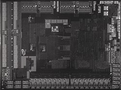 Infrared die shot of the I/O Die
 EPYC I/O Die
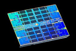 Zen 2 Core Complex Die (CCD)
 AMD EPYC 7702 server processor
 A delidded AMD 7702 featuring 8 CCDs and 1 I/O die, with remains of the solder thermal interface material (TIM) on the chiplets

@Zen2@Matisse@Ryzen_5_3600@100-000000031_BF_1923SUT_9HM6935R90062_DSC04789-DSC04810_-_ZS-DMap_(48319202011).jpg)
@Zen2@Matisse@Ryzen_5_3600@100-000000031_BF_1923SUT_9HM6935R90062_DSCx4@IOD_Infrared.jpg)


@Zen2@Rome@EPYC_7702_ES@2S1404E2VJUG5_BB_ES_DSCx1.jpg)
@Zen2@Rome@EPYC_7702_ES@2S1404E2VJUG5_BB_ES_DSCx3.jpg)
See also
Wikimedia Commons has media related to Zen 2 microarchitecture.
References
Wikiwand - on
Seamless Wikipedia browsing. On steroids.
Remove ads