StrongARM
Family of computer microprocessors From Wikipedia, the free encyclopedia
The StrongARM is a family of computer microprocessors developed by Digital Equipment Corporation and manufactured in the late 1990s which implemented the ARM v4 instruction set architecture.[1] It was later acquired by Intel in 1997 from DEC's own Digital Semiconductor division as part of a settlement of a lawsuit between the two companies over patent infringement.[2] Intel then continued to manufacture it before replacing it with the StrongARM-derived ARM-based follow-up architecture called XScale in the early 2000s.

History
Summarize
Perspective
According to Allen Baum, the StrongARM traces its history to attempts to make a low-power version of the DEC Alpha, which DEC's engineers quickly concluded was not possible. They then became interested in designs dedicated to low-power applications which led them to the ARM family. One of the only major users of the ARM for performance-related products at that time was Apple, whose Newton device was based on the ARM platform. DEC approached Apple wondering if they might be interested in a high-performance ARM, to which the Apple engineers replied "Phhht, yeah. You can't do it, but, yeah, if you could we'd use it."[3]
The StrongARM was a collaborative project between DEC and Advanced RISC Machines to create a faster ARM microprocessor. The StrongARM was designed to address the upper end of the low-power embedded market, where users needed more performance than the ARM could deliver while being able to accept more external support. Targets were devices such as newer personal digital assistants and set-top boxes.[4][5]
Traditionally, the semiconductor division of DEC was located in Massachusetts. In order to gain access to the design talent in Silicon Valley, DEC opened a design center in Palo Alto, California. This design center was led by Dan Dobberpuhl and was the main design site for the StrongARM project. Another design site that worked on the project was in Austin, Texas that was created by some ex-DEC designers returning from Apple Computer and Motorola. The project was set up in 1995, and quickly delivered their first design, the SA-110.
DEC agreed to sell StrongARM to Intel as part of a lawsuit settlement in 1997.[6] Intel used the StrongARM to replace their ailing line of RISC processors, the i860 and i960.
When the semiconductor division of DEC was sold to Intel, many engineers from the Palo Alto design group moved to SiByte, a start-up company designing MIPS system-on-a-chip (SoC) products for the networking market. The Austin design group spun off to become Alchemy Semiconductor, another start-up company designing MIPS SoCs for the hand-held market. A new StrongARM core was developed by Intel and introduced in 2000 as the XScale.[7]
SA-110
Summarize
Perspective
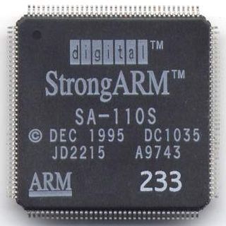
The SA-110 was the first microprocessor in the StrongARM family. The first versions, operating at 100, 160, and 200 MHz, were announced on 5 February 1996.[8] When announced, samples of these versions were available, with volume production slated for mid-1996. Faster 166 and 233 MHz versions were announced on 12 September 1996.[9] Samples of these versions were available at announcement, with volume production slated for December 1996. Throughout 1996, the SA-110 was the highest performing microprocessor for portable devices.[10] Towards the end of 1996 it was a leading CPU for internet/intranet appliances and thin client systems.[11] The SA-110's first design win was the Apple MessagePad 2000.[12] It was also used in a number of products including the Acorn Computers Risc PC and Eidos Optima video editing system. The SA-110's lead designers were Daniel W. Dobberpuhl, Gregory W. Hoeppner, Liam Madden, and Richard T. Witek.[4]
Description
The SA-110 had a simple microarchitecture. It was a scalar design that executed instructions in-order with a five-stage classic RISC pipeline. The microprocessor was partitioned into several blocks, the IBOX, EBOX, IMMU, DMMU, BIU, WB and PLL. The IBOX contained hardware that operated in the first two stages of the pipeline such as the program counter. It fetched, decoded and issued instructions. Instruction fetch occurs during the first stage, decode and issue during the second. The IBOX decodes the more complex instructions in the ARM instruction set by translating them into sequences of simpler instructions. The IBOX also handled branch instructions. The SA-110 did not have branch prediction hardware, but had mechanisms for their speedy processing.
Execution starts at stage three. The hardware that operates during this stage is contained in the EBOX, which comprises the register file, arithmetic logic unit (ALU), barrel shifter, multiplier and condition code logic. The register file had three read ports and two write ports. The ALU and barrel shifter executed instructions in a single cycle. The multiplier is not pipelined and has a latency of multiple cycles.
The IMMU and DMMU are memory management units for instructions and data, respectively. Each MMU contained a 32-entry fully associative translation lookaside buffer (TLB) that can map 4 KB, 64 KB or 1 MB pages. The write buffer (WB) has eight 16-byte entries. It enables the pipelining of stores. The bus interface unit (BIU) provided the SA-110 with an external interface.
The PLL generates the internal clock signal from an external 3.68 MHz clock signal. It was not designed by DEC, but was contracted to the Centre Suisse d'Electronique et de Microtechnique (CSEM) located in Neuchâtel, Switzerland.
The instruction cache and data cache each have a capacity of 16 KB and are 32-way set-associative and virtually addressed. The SA-110 was designed to be used with slow (and therefore low-cost) memory and therefore the high set associativity allows a higher hit rate than competing designs, and the use of virtual addresses allows memory to be simultaneously cached and uncached. The caches are responsible for most of the transistor count and they take up half the die area.
The SA-110 contained 2.5 million transistors and is 7.8 mm by 6.4 mm large (49.92 mm2). It was fabricated by DEC in its proprietary CMOS-6 process at its Fab 6 fab in Hudson, Massachusetts. CMOS-6 was DEC's sixth-generation complementary metal–oxide–semiconductor (CMOS) process. CMOS-6 has a 0.35 μm feature size, a 0.25 μm effective channel length but for use with the SA-110, only three levels of aluminium interconnect. It used a power supply with a variable voltage of 1.2 to 2.2 volts (V) to enable designs to find a balance between power consumption and performance (higher voltages enable higher clock rates). The SA-110 was packaged in a 144-pin thin quad flat pack (TQFP).
SA-1100
Summarize
Perspective
The SA-1100 was a derivative of the SA-110 developed by DEC. Announced in 1997, the SA-1100 was targeted for portable applications such as PDAs and differs from the SA-110 by providing a number of features that are desirable for such applications. To accommodate these features, the data cache was reduced in size to 8 KB.
The extra features are integrated memory, PCMCIA, and color LCD controllers connected to an on-die system bus, and five serial I/O channels that are connected to a peripheral bus attached to the system bus. The memory controller supported FPM and EDO DRAM, SRAM, flash, and ROM. The PCMCIA controller supports two slots. The memory address and data bus is shared with the PCMCIA interface. Glue logic is required. The serial I/O channels implement a slave USB interface, a SDLC, two UARTs, an IrDA interface, a MCP, and a synchronous serial port.
The SA-1100 had a companion chip, the SA-1101. It was introduced by Intel on 7 October 1998.[13] The SA-1101 provided additional peripherals to complement those integrated on the SA-1100 such as a video output port, two PS/2 ports, a USB controller and a PCMCIA controller that replaces that on the SA-1100. Design of the device started by DEC, but was only partially complete when acquired by Intel, who had to finish the design. It was fabricated at DEC's former Hudson, Massachusetts fabrication plant, which was also sold to Intel.[14]
The SA-1100 contained 2.5 million transistors and measured 8.24 mm by 9.12 mm (75.15 mm2). It was fabricated in a 0.35 μm CMOS process with three levels of aluminium interconnect and was packaged in a 208-pin TQFP.[15]
One of the early recipients of this processor was-ill-fated Psion netBook and its more consumer oriented sibling Psion Series 7.
SA-1110
The SA-1110 was a derivative of the SA-110 developed by Intel. It was announced on 31 March 1999, positioned as an alternative to the SA-1100.[16] At announcement, samples were set for June 1999 and volume later that year. Intel discontinued the SA-1110 in early 2003.[17] The SA-1110 was available in 133 or 206 MHz versions. It differed from the SA-1100 by featuring support for 66 MHz (133 MHz version only) or 103 MHz (206 MHz version only) SDRAM.[18] Its companion chip, which provided additional support for peripherals, was the SA-1111. The SA-1110 was packaged in a 256-pin micro ball grid array. It was used in mobile phones, personal data assistants (PDAs) such as the Compaq (later HP) iPAQ and HP Jornada, the Sharp SL-5x00 Linux Based Platforms and the Simputer.[19] It was also used to run the Intel Web Tablet, a tablet device that is considered potentially the first to introduce large screen, portable web browsing. Intel dropped the product just prior to launch in 2001.
SA-1500
Summarize
Perspective
The SA-1500 was a derivative of the SA-110 developed by DEC initially targeted for set-top boxes.[20][21] It was designed and manufactured in low volumes by DEC but was never put into production by Intel. The SA-1500 was available at 200 to 300 MHz. The SA-1500 featured an enhanced SA-110 core, an on-chip coprocessor called the Attached Media Processor (AMP), and an on-chip SDRAM and I/O bus controller. The SDRAM controller supported 100 MHz SDRAM, and the I/O controller implemented a 32-bit I/O bus that may run at frequencies up to 50 MHz for connecting to peripherals and the SA-1501 companion chip.
The AMP implemented a long-instruction-word instruction set containing instructions designed for multimedia, such as integer and floating-point multiply–accumulate operations and SIMD arithmetic. Each long-instruction word is 64 bits wide and specifies an arithmetic operation and a branch or a load/store. Instructions operate on operands from a 64-entry 36-bit register file, and on a set of control registers. The AMP communicates with the SA-110 core via an on-chip bus and it shares the data cache with the SA-110. The AMP contained an ALU with a shifter, a branch unit, a load/store unit, a multiply–accumulate unit, and a single-precision floating-point unit. The AMP supported user-defined instructions via a 512-entry writable control store.[22]
The SA-1501 companion chip provided additional video and audio processing capabilities and various I/O functions such as PS/2 ports, a parallel port, and interfaces for various peripherals.
The SA-1500 contains 3.3 million transistors and measures 60 mm2. It was fabricated in a 0.28 μm CMOS process. It used a 1.5 to 2.0 V internal power supply and 3.3 V I/O, consuming less than 0.5 W at 100 MHz and 2.5 W at 300 MHz. It was packaged in a 240-pin metal quad flat package or a 256-ball plastic ball grid array.
StrongARM latch
The StrongARM latch is an electronic latch circuit topology first[23][24] proposed by Toshiba engineers Tsuguo Kobayashi et al.[25] and got significant attention after being used in StrongARM microprocessors.[23][24] It is widely used as a sense amplifier, a comparator, or just a robust latch with high sensitivity.[23][24]
References
Further reading
Wikiwand - on
Seamless Wikipedia browsing. On steroids.
