Top Qs
Timeline
Chat
Perspective
Floorplan (microelectronics)
Layout of major electronic circuit blocks From Wikipedia, the free encyclopedia

Remove ads
In electronic design automation, a floorplan of an integrated circuit consists of a schematic arrangement of its major functional blocks on the chip area and the specification of high-level parameters such as the aspect ratio or core utilization.[1]
The design step in which floorplans are created is called floorplanning, an early stage in the design flow for integrated circuit design.[1]
Various mathematical abstractions of this problem have been studied.[2]
Remove ads
Floorplanning design stage
Summarize
Perspective
The floorplanning design stage consists of various steps with the aim of finding floorplans that allow a timing-clean routing and spread power consumption over the whole chip.
- Chip Area Estimation: The dimensions and aspect ratio of the chip area are determined. The estimation considers the space required to place macros, standard cells and I/O ports while also leaving enough space for routing resources to enable a successful place and route design flow. Usually a core utilization of 60%-70% is targeted.[3]

- I/O Pad Positioning: Input/Output Pads usually need to be positioned along the periphery of the chip. Near the I/O Pads space for line drivers needs to be reserved to minimize delay and signal degradation.[4]
- Macro Placement: During macro placement large functional blocks with a fixed size and fixed pins such as memory arrays, clock generators or custom components need to be placed within the floorplan's outline. Effective macro placement minimizes the length of timing critical paths, avoids routing congestion and ensures thermal balance.[4]
- Standard Cell Row Creation: Areas where standard cells should be placed are determined and divided into standard cell rows. During the placement stage standard cells are forced to align with standard cell rows[5] although they might be of multi-row height. The height of the standard cell rows determines the available routing resources per row while also influencing the power.[6]
Remove ads
Mathematical models
In mathematics floorplanning refers to the problem of packing smaller rectangles with a fixed or unfixed orientation into a larger rectangle.[citation needed] The dimensions of the larger and smaller rectangles might be fixed (hard constraints) or must be optimized (soft constraints). Additionally, a measure modelling the quality of routing that the floorplan allows might be optimized.
Various variants of rectangle packing are NP-hard.[8]
Remove ads
Sliceable floorplans
A sliceable floorplan is a floorplan that may be defined recursively as described below.[9]
- A floorplan that consists of a single rectangular block is sliceable.
- If a block from a sliceable floorplan is cut ("sliced") in two by a vertical or horizontal line, the resulting floorplan is sliceable.
The process is known as guillotine cutting. Sliceable floorplans have been used in a number of early electronic design automation tools[9] for a number of reasons. Sliceable floorplans may be conveniently represented by binary trees (more specifically, k-d trees), which correspond to the order of slicing. More importantly, a number of NP-hard problems with floorplans have polynomial time algorithms when restricted to sliceable floorplans.[10]
 A sliceable floorplan
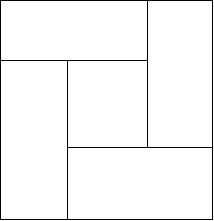 A non-sliceable floorplan


Further reading
- The Chip Planner of the PLAYOUT System
- VLSI Physical Design: From Graph Partitioning to Timing Closure, by Kahng, Lienig, Markov and Hu, doi:10.1007/978-3-030-96415-3ISBN 978-3-030-96414-6, 2022
- Fundamentals of Layout Design for Electronic Circuits, by Lienig, Scheible, Springer, doi:10.1007/978-3-030-39284-0ISBN 978-3-030-39284-0, 2020
References
Wikiwand - on
Seamless Wikipedia browsing. On steroids.
Remove ads