Loading AI tools
From Wikipedia, the free encyclopedia
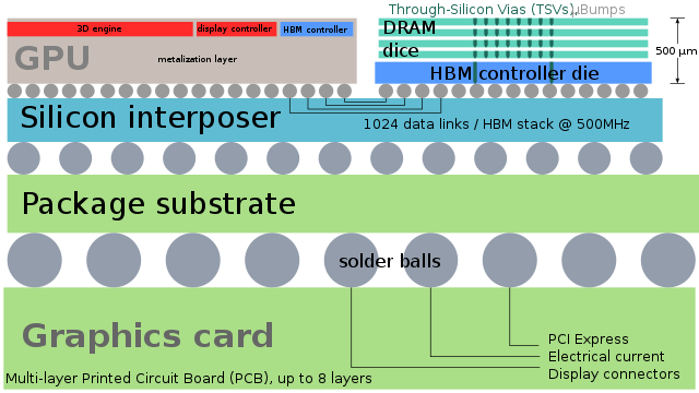
In integrated circuit packaging, a solder ball, also a solder bump (often referred to simply as "ball" or "bumps") is a ball of solder that provides the contact between the chip package and the printed circuit board, as well as between stacked packages in multichip modules;[1] in the latter case, they may be referred to as microbumps (μbumps, ubumps), since they are usually significantly smaller than the former. The solder balls can be placed manually or by automated equipment, and are held in place with a tacky flux.[2]


A coined solder ball is a solder ball subject to coining, i.e., flattening to a shape resembling that of a coin, to increase contact reliability.[3]
The ball grid array, chip-scale package, and flip chip packages generally use solder balls.
After the solder balls are used to attach an integrated circuit chip to a PCB, often the remaining air gap between them is underfilled with epoxy.[4][5]
In some cases, there may be multiple layers of solder balls—for example, one layer of solder balls attaching a flip chip to an interposer to form a BGA package, and a second layer of solder balls attaching that interposer to the PCB. Often both layers are underfilled.[6][7]
Seamless Wikipedia browsing. On steroids.
Every time you click a link to Wikipedia, Wiktionary or Wikiquote in your browser's search results, it will show the modern Wikiwand interface.
Wikiwand extension is a five stars, simple, with minimum permission required to keep your browsing private, safe and transparent.